[#小町戯言シリーズ] 6/15~6/23 Tweet Summary.
1.CometLake/IceLake/LakeField Info.
*Con


5.AMD Athlon 300GE.
適当にまとめておきました。気になる人は見てね。https://t.co/HdLz0aCQEv— 比屋定さんの戯れ言@Komachi (@KOMACHI_ENSAKA) 2019年6月16日
There are three versions of CML-U.
V0 / S0 / K0 exists, but V0 is the same as the current WHL-U.
Also, the difference between S0 and K0 is whether it is a 4 + 2 die or a 6 + 2 die.
V0 / S0 / K0 exists, but V0 is the same as the current WHL-U.
Also, the difference between S0 and K0 is whether it is a 4 + 2 die or a 6 + 2 die.
*Con
WHL-U = V0 & W0 Stepping (V0 Stepping adds hardware level vulnerability measures to V2/V3/V4/L1TF/MFBDS/MSBDS/MLPDS/MDSUM)
CML-U = K0 (6+2) & V0/S0 (4+2)
CML-H/S = P0 (10+2 or 6+2) & G0 (10+2 or 6+2).
LKF GT1 = 8×8 (64EU / 512SP).
2.AMD Navi 10 RDNA vs AMD Vega 10 GCN.
"Navi 10 with 40 CU" and "Vega 10 with 40 CU" comparison is not for performance comparison but for power comparison. https://t.co/Vql7RHE7Po— 比屋定さんの戯れ言@Komachi (@KOMACHI_ENSAKA) 2019年6月17日
AMD seems to use "40 CU enabled Navi 10" and "40 CU enabled Vega 10" for power efficiency comparison of RDNA μArch and GCN μArch.
It is used for power efficiency comparison only, and for performance comparison, "Navi 10 (40 CU)" and "Vega 10 (64 CU)" are used.
* (The clock is unknown. Not stated in the end note. Not stated in the E3/Computex documents.)
It is used for power efficiency comparison only, and for performance comparison, "Navi 10 (40 CU)" and "Vega 10 (64 CU)" are used.
* (The clock is unknown. Not stated in the end note. Not stated in the E3/Computex documents.)
Note.
Navi 10 = 40CU : 256bit memory Bus : GDDR6 8GB : 251mm2 : TSMC 7nm.
Vega 10 = 64CU : 2048bit memory Bus : HBM2 8GB : 486mm2 (495mm2*) : GF 14nm.
*AMD doesn't specify the Vega 10 die size. They are using 486mm2 and 495mm2.
3.AMD Navi 10 Story.
drm/amdgpu/mes: add amdgpu_mes driver parameter https://t.co/Lqq2N2pT05— 比屋定さんの戯れ言@Komachi (@KOMACHI_ENSAKA) 2019年6月18日
>MES (Micro Engine Scheduler) is the new on chip hw scheduling
microcontroller. It can be used to handle queue scheduling and
preemption and priorities.
The MES (Micro Engine Scheduler) is probably an evolution of the "Hardware Scheduler," which is installed on current GCN cards.
The current GCN GPU has two HWSs, but the RDNA-based Navi 10 has one.
(The HWS is installed from the Fiji XT / Fury Series (GFX 803). Officially, it is from the Polaris (GFX 803/804), but as far as I know., First statement is the Hotchips announcement about Fiji.)
The current GCN GPU has two HWSs, but the RDNA-based Navi 10 has one.
(The HWS is installed from the Fiji XT / Fury Series (GFX 803). Officially, it is from the Polaris (GFX 803/804), but as far as I know., First statement is the Hotchips announcement about Fiji.)
Reference
*AMD Vega 10 Block Diagram & AMD Navi 10 Block Diagram.


drm/amdgpu: disable concurrent flushes for Navi10 v2 https://t.co/8tlwj3wKbK— 比屋定さんの戯れ言@Komachi (@KOMACHI_ENSAKA) 2019年6月18日
>/* Concurrent flushes are only possible starting with Vega10 and * are broken on Navi10 and Navi14.
Here We can see that Navi 10 and Navi 14 have the same hardware-induced bugs.
As I said before in twitter, the order of appearance of Navi should be Navi 10 → Navi 14 → Navi 12 → Navi 21. It will be a form that can be reconfirmed from here.
As I said before in twitter, the order of appearance of Navi should be Navi 10 → Navi 14 → Navi 12 → Navi 21. It will be a form that can be reconfirmed from here.
[KOMACHI] GFX1012 = NAVI14. GFX101F = NAVI10_A0. pic.twitter.com/zlY0BQN4ac— 比屋定さんの戯れ言@Komachi (@KOMACHI_ENSAKA) 2019年6月18日
The table created based on this tweet is here.
[KOMACHI] AMD GPU Table for Vega & Navi Version 2.1.1.1 (6/18/2019) pic.twitter.com/ONRHUmvrEs— 比屋定さんの戯れ言@Komachi (@KOMACHI_ENSAKA) 2019年6月18日


Although I didn't tweet too much, PCI-ID arrangement of Navi 10 LITE is in the part of APU/iGPU. It should not be dGPU.
4.AMD EPYC 7002 Series & AMD Ryzen 3000G Series.
[EEC] AMD EPYC 7002 Series. https://t.co/xBj70IolFz pic.twitter.com/Se6zJRxZCG— 比屋定さんの戯れ言@Komachi (@KOMACHI_ENSAKA) 2019年6月18日
AMD EPYC 7002 Series (Rome) Table. pic.twitter.com/Op0F0eTftF— 比屋定さんの戯れ言@Komachi (@KOMACHI_ENSAKA) 2019年6月18日
[EEC] AMD PICASSO DT (Ryzen 3400G/E & 3200G/E) https://t.co/34wEgzq0ct— 比屋定さんの戯れ言@Komachi (@KOMACHI_ENSAKA) 2019年6月18日
>3400GE 35W. 3200GE 35W. pic.twitter.com/Y3fOp19c6N
7320P should be 7302P.
I also heard that there is no 12C SKU.
I also heard that there is no 12C SKU.
5.AMD Athlon 300GE.
Memo: Athlon 300GE : RAVEN2 : 2C4T w/ Vega 3 Graphics @ 1100Mhz (1101?).— 比屋定さんの戯れ言@Komachi (@KOMACHI_ENSAKA) 2019年6月18日
It is basically the same as the current Athlon 200 Series, but the CPU part has been updated to Zen +, and the GPU part has been updated to GFX909.
It is important to note here that it is based on a die called RAVEN2, so unlike 200 series based on RAVEN1, unlocking of PCI-E lanes etc. is not possible.
Also, unlike PICASSO, it is manufactured at 14 nm rather than 12 nm.
It is important to note here that it is based on a die called RAVEN2, so unlike 200 series based on RAVEN1, unlocking of PCI-E lanes etc. is not possible.
Also, unlike PICASSO, it is manufactured at 14 nm rather than 12 nm.
6.AMD A320 M/B.
[BIOSTAR] A320 BIOS Update (6/X/2019)— 比屋定さんの戯れ言@Komachi (@KOMACHI_ENSAKA) 2019年6月19日
A320MH PRO BIOS-A32AS603.BSS.
A320MY-Q7 BIOS-A32ES523.1PS.
A320MH BIOS-A32ES520.BSS.
A320MD PRO BIOS-A32BS603.BSS.
1. Update AGESA ComboAM4 PI 1.0.0.1.
2. Support Ryzen 3000 Series CPU (MTS-A0 & MTS-B0).
AMD has officially stated that the A320 chipset does not support "Matisse / MTS (Ryzen 3000 Series CPU)", but ASUS and BIOSTAR have issued BIOS that supports MTS.
There should be no technical problems, so I think that depending on the manufacturer, it means to respond.
It is unclear whether other companies will follow.
Reference
GeekBench 4 : Ryzen 5 3600 + ASUS A320M-K/AGESA 0.0.7.2A or Higher.
URL : https://browser.geekbench.com/v4/cpu/13609546
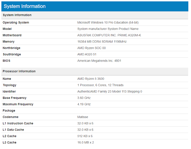
GeekBench 4 : Ryzen 5 3600 + ASUS A320M GAMING/AGESA 0.0.7.2A.
URL : https://browser.geekbench.com/v4/cpu/13609975

7. AMD Navi 10 PCI-ID.
[GFXBench] 3D Graphics Performance of AMD 731F:C1 https://t.co/kg9fQKU7YU— 比屋定さんの戯れ言@Komachi (@KOMACHI_ENSAKA) 2019年6月20日
Navi 10!
[GPU-Z] GPU-Z Validation : RX 5700 (731F:C4 : Navi 10 Pro).https://t.co/cGlGsOyIvb— 比屋定さんの戯れ言@Komachi (@KOMACHI_ENSAKA) 2019年6月22日
(All Spec are displayed in Half. Because GPU-Z doesn't support RDNA GPU yet) pic.twitter.com/66FOwLouWU
Con.
7310~731F = Navi 10 ID.
7310 = WorkStation Card (WX Series or Radeon Instinct).
731F = CS Card (RX 5700 Series).
731F:C1 = XT (XTX).
731F:C4 = Pro.
Thank you ;)
コメント
コメントを投稿